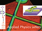
Molecular electronics offers the tantalizing prospect of eventually
building circuits with critical dimensions of a few nanometers.
Some basic devices utilizing molecules have been demonstrated,
including tunnel junctions with negative differential resistance,
rectifiers and electrically configurable switches that have
been used in simple electronic memory and logic circuits. A
major challenge that remains is to show that such devices can
be fabricated economically using a process that will scale to
circuits with large numbers of elements while maintaining their
desired electronic properties.
» Read the full paper.
» Requires
Adobe Acrobat.
Authors:
- Yong Chen, Douglas A. A. Ohlberg, Xuema Li, Duncan R.
Stewart, and R. Stanley Williams Quantum
Science Research, Hewlett-Packard Laboratories
- Jan O. Jeppesen, Kent A. Nielsen, and J. Fraser Stoddart,
Department of Chemistry and Biochemistry and The California
NanoSystems Institute, University of California, Los Angeles
- Deirdre L. Olynick and Erik Anderson, Lawrence Berkeley
National Laboratory
More about the HP Labs authors:
 Yong Chen is a senior scientist at HP Labs, working in
the area of molecular electronics. He received his PhD in
Materials Science (Minor, Electrical Engineering) from the
University of California, Berkeley. Before joining HP, he
worked at the National Laboratory of Solid State Microstructures,
Nanjing University, P.R.China, and at Lawrence Berkeley National
Laboratories, University of California. In 2002, he was among
those named to the inaugural "Scientific American 50."
Yong Chen is a senior scientist at HP Labs, working in
the area of molecular electronics. He received his PhD in
Materials Science (Minor, Electrical Engineering) from the
University of California, Berkeley. Before joining HP, he
worked at the National Laboratory of Solid State Microstructures,
Nanjing University, P.R.China, and at Lawrence Berkeley National
Laboratories, University of California. In 2002, he was among
those named to the inaugural "Scientific American 50."
 Xuema Li is a process engineer at HP
Labs. She jointed the Quantum Science Research Lab in 2000,
and has been working on nano fabrication of semiconductor
materials. She is interested in a variety of processes, which
include RIE etching, e-beam and optical lithography, CVD growing
and film deposition. She has a MS degree in Material Science.
Xuema Li is a process engineer at HP
Labs. She jointed the Quantum Science Research Lab in 2000,
and has been working on nano fabrication of semiconductor
materials. She is interested in a variety of processes, which
include RIE etching, e-beam and optical lithography, CVD growing
and film deposition. She has a MS degree in Material Science.
Doug A. A. Ohlberg received a BS in chemistry in 1989
from California State University, Fresno. His MS in chemistry
was obtained in 1995 at the University of California, Los
Angeles, with R. Stanley Williams (now director of the Quantum
Science Research Lab) as his advisor. From 1994 to 1996, he
worked as a Graduate Fellow for Sandia National Laboratories
in the flat panel display initiative. He joined the Quantum
Structures Research Initiative at Hewlett-Packard as an R&D
specialist in 1996.
 Duncan Stewart is a researcher at Hewlett-Packard Laboratories,
investigating the physics of molecular electronic transport
and devices. He received a BASc in Engineering Physics from
the University of Toronto in 1992, and a PhD in Applied Physics
from Stanford University in 1999. He joined the Quantum Science
Research group, directed by Stan Williams, in September 1999.
Duncan Stewart is a researcher at Hewlett-Packard Laboratories,
investigating the physics of molecular electronic transport
and devices. He received a BASc in Engineering Physics from
the University of Toronto in 1992, and a PhD in Applied Physics
from Stanford University in 1999. He joined the Quantum Science
Research group, directed by Stan Williams, in September 1999.
 Stan Williams is a Senior HP
Fellow and director of Quantum Science Research at HP
Labs, conducting research into nanoscale science and the fundamental
physics of switching, with an emphasis on molecular electronics.
His research interests are in the areas of solid-state chemistry
and physics and their application to technology. His awards
for scientific and academic achievement include the Dreyfus
Teacher-Scholar Award, the Sloan Foundation Fellowship, the
Julius Springer Award for Applied Physics and the Feynman
Prize in Nanotechnology. In 2002, Williams was among those
named to the inaugural "Scientific American 50."
Stan Williams is a Senior HP
Fellow and director of Quantum Science Research at HP
Labs, conducting research into nanoscale science and the fundamental
physics of switching, with an emphasis on molecular electronics.
His research interests are in the areas of solid-state chemistry
and physics and their application to technology. His awards
for scientific and academic achievement include the Dreyfus
Teacher-Scholar Award, the Sloan Foundation Fellowship, the
Julius Springer Award for Applied Physics and the Feynman
Prize in Nanotechnology. In 2002, Williams was among those
named to the inaugural "Scientific American 50."
Applied Physics Letters copyright notice:
This paper is reprinted with permission from Applied Physics
Letters, March 10, 2003 -- Volume 82, Issue 10, pp. 1610-1612,
© 2003, American Institute of Physics.
This article may be downloaded for personal use only. Any
other use requires prior permission of the authors and the
American Institute of Physics (rights@aip.org)
|