|
|
 |
» |
|
| |
 |
|
|
|
|
| |
Optical fibers have revolutionized telecommunications, communicating signals over long distances for telephone and television systems and the Internet, as well as providing the backbones for many public and private network systems.
They are lighter and thinner than equivalent lengths of copper wire, and they can carry more data at higher speeds. Not only does copper wire generate more heat than optical fiber, but the wire can carry only one signal at a time, while many optical signals can be ‘multiplexed’ onto a single optical fiber.
Copper remains dominant for the shorter-distance communications inside microprocessors, servers and data centers, primarily because of cost. Historically, the infrastructure to support an optical fiber network has been expensive, so optics has been used to communicate information only over long distances, from hundreds of meters to kilometers.
During the past decade, the field of opto-electronics has seen dramatic reductions in the cost of the components of an optical data transmission network, and now optical networks that communicate at distances of 10 to 100 meters are becoming practical.
Growing demands for computing bandwidth and power have resulted in increasingly dense microprocessors and computing systems, leading to the ‘multicore’ era. Yet because copper wire can carry only one signal at a time, there is simply not enough room on a computer chip to connect all of the transistors in an efficient way.
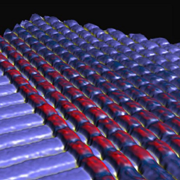
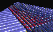
During the past few years, advances in the field of nanophotonics – leading to the creation of optical ‘waveguides’ (optical conduits similar to fiber, but less than one micrometer wide) – have raised the possibility that optics can replace metal interconnects over distances as short as one millimeter.
Our scientists are working to replace copper wire interconnects with optical interconnects over distances from 10 meters (in room-size computer networks) down to 1 mm (on computer chips) using inexpensive silicon-based fabrication technology that has been the mainstay of the computer industry for 40 years.
If we can accomplish this, we can reduce the amount of heat these systems generate and potentially cut energy use in half. |
|
 |
| |
|
Replacing copper wire interconnects with optical interconnects may reduce heat generated by everything from computer chips to room-size computer networks – and cut power use in half. |
|
| |
|
|
|
Our research into nanophotonics produced an unexpected realization that some of the structures we developed for data communications systems might also be applied to creating potentially highly efficient, low-cost solar cells.
The structures incorporate III-V nanowires on silicon for ultra-high speed devices such as photodectors that convert light to electricity. These devices can use light – rather than copper -- to move data within the computer at billions of bits per second.
By changing the device structures slightly, we may be able to apply the same to solar cells using a thin film process that can be fabricated at very low cost. This work is continuing.
|
|
|
| |
|
|
Computing systems, especially in data centers, use energy for three primary functions: moving data around between disk, memory and the processor core, operating ondata logically, and for a huge portion of time, doing nothing.
Computing systems are specified for peak loading, but much of the time they operate at much lower loads. Yet slow on/off times make it impractical to shut down many under-utilized sub-systems.
HP's nano-crossbar memories can dramatically reduce power required for ‘doing nothing’ by providing a fast, low-power, non-volatile memory technology for instant-on service. A non-volatile memory remembers its state even with zero power supplied. Inside a single computer -- and even on a single chip -- each computing component turns on only long enough to get the job done.
With non-volatile memories, data center operators are free to turn things off because turning them back on is instantaneous. The result: enormous power savings, especially for larger high- performance systems.
The nano-crossbar memories can also significantly reduce operating power by integrating a huge data cache on every logic chip. This eliminates slow, often redundant, high-power communications between the processor and separate memory chips.
|
|
|
| |
|
|
Large networks of smart, cheap sensors will make it possible to use many resources more efficiently. Already, sensors can turn the lights, air conditioning or heating on or off in a building or room by detecting when people are present.
In the future, sensors could help farmers measure the soil and crops to prevent over-watering and fertilizing. Or they could help manage the infrastructure of buildings, roads and bridges by measuring structural decay to limit overuse or to schedule needed maintenance.
Unfortunately, most existing sensors require large batteries – and changing the batteries on thousands of chip-scale sensors across a network is simply not feasible.
HP's nano-crossbar memory is designed to enable these distributed devices to operate in the most efficient way -- they will wake up, take a measurement, make a decision, communicate if necessary, store the result, and go back to a zero-power sleep. Power requirements will be small enough to enable on-chip batteries to last a lifetime.
Even more exciting, keeping power requirements low may make it possible to harvest the needed energy from the sensor surroundings such as solar light, heat cycles or vibrations -- eliminating the need for any batteries at all.
HP Labs is applying its nanocrossbar memory to developing nanosensor technologies designed to allow instant identification and analysis of a biological or environmental hazard or change.
|
|
 |
| |
|
Efficient use of any resource electricity, water, soil, or even roads and bridges -- requires careful monitoring and control. Better monitoring requires large networks of smart, cheap sensors. Such a large sensor network is only possible with ultra low-power chip-scale devices. |
|
| |
|
| |
|
|
For decades, increases in chip performance have come about largely by shrinking transistors and wires to pack more power into a smaller space. But transistors can only get so small before problems of heat generation, defects and basic physics get in the way.
Scientists may have found a way around this with an architecture called field programmable nanowire interconnect (FPNI). FPNI combines a nanoscale crossbar switch structure with conventional CMOS to create a hybrid chip with higher density -- while requiring less power and generating less heat. (See related feature: A novel way to better chips.)
FPNI is a variation on field-programmable gate arrays (FPGA), a type of integrated circuit that can be adapted by end users for specific applications.
Because the new chips would use the same-sized transistors as those used in existing FPGA designs, they could be manufactured in existing fabrication facilities with only minor modifications.
The researchers avoided shrinking transistors by removing the wiring and switches between the logic cells on the silicon layer of the FPGA -- leaving more room for logic gates and allowing them to be placed closer together. The wiring and switches are replaced by a nanoscale crossbar switch structure that performs the same functions but resides in a layer above the transistors.
They believe a similar concept for placing switches in the interconnect wiring could be applied to other types of integrated circuits. They are used in a wide range of industries, including communications, automotive and consumer electronics.
The new architecture could help extend Moore’s Law (by which manufacturers have continually increased the capacity of chips) for several decades rather than running out in the next decade as many have expected.
|
|
 |
| |
|
Researchers have demonstrated a new way to produce configurable chips that use less energy and provide up to eight times the density at lower cost. Their design could help extend the physical limits of Moore’s Law. |
|
| |
|
| |
|
